Table of Contents
gEDA Project Wiki
What is gEDA?
Translations: Français, Español, Русский
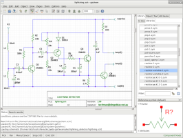
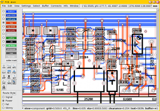
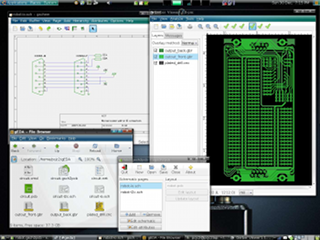
The gEDA project is developing a full GPL'd suite and toolkit of Electronic Design Automation tools. These tools are used for electrical circuit design, schematic capture, simulation, prototyping, and production. Currently, the gEDA project offers a mature suite of free software applications for electronics design, including schematic capture, attribute management, bill of materials (BOM) generation, netlisting into over 20 netlist formats, analog and digital simulation, and printed circuit board (PCB) layout.
The tools involved in the suite enable you to professional-quality design of low- to mid-level complexity. Using the gEDA tools, you can create PCB of up to 8 layers (soon more) with an unlimited number of components and nets. The tools are suitable for use by students, educators, hobbyists, consultants, small businesses, and even in large corporations where an engineer might need to crank out a quick PC board (e.g. for a test stand) in a hurry.
Frequently asked questions
Community
Users may discuss development, help, installation, and working tips through the mailinglists.
There is also a gEDA IRC channel at irc.oftc.net/6667 on the #geda channel. This is the official IRC channel for all things gEDA. Sometimes this channel is full of activity and sometimes it is quite silent. Please be patient when asking questions in the IRC channel.
There is also a low-traffic IRC channel on irc.freenode.net called ##pcb. This channel is dedicated to pcb design and prototyping, gEDA pcb included.


